Research
Femtosecond Laser Waveguide Inscription
The discovery that focussed femtosecond pulses can generate positive refractive index modifications inside materials by Davis et al in 1996 [1] has generated substantial research interest in using femtosecond lasers to fabricate integrated optical devices. The material is simply translated through the focus of the pulse train to effectively 'write' a waveguide inside the bulk medium.
 At the heart of the refractive index modification process is a highly nonlinear multi-photon mechanism, which is not entirely understood at this time. Nevertheless, the technique has been applied very successfully to the fabrication of a wide range of devices. As the modification process is highly nonlinear, the modified region is highly localised to a small area around the focus of the femtosecond pulse train. This enables 3-dimensional structures to be fabricated with relative ease, a capability unique to this fabrication technique.
There are two distinct regimes for waveguide fabrication, dependant upon the repetition rate of the fabrication laser. In the low repetition rate regime (<1MHz) the index modification mechanism is thought to be a result of energy transfer to the material lattice from the microplasma generated in the focal region. Waveguides fabricated in the low repetition rate regime suffer from a high level of asymmetry unless corrective steps are employed. In the High repetition rate regime (>1MHz) the inter-pulse duration is shorter than the thermal diffusion time, leading to a cumulative heating effect which modifies the material through a localised thermal annealing. This regime however does not appear to work for many materials, and is less flexible as it requires very high NA objective lenses with short working distances, greatly reducing the 3 dimensional fabrication capability.
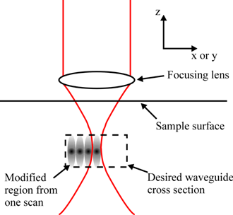
Working in the low repetition rate regime is therefore of greater interest, using corrective methods to control the waveguide cross section. Thus far, three techniques [2,3,4] have been suggested for fabricated waveguides with symmetric cross section while remaining in the low repetition rate regime. To date, we have focussed on the multi-scan technique since it is the most flexible of the proposed methods. In the multi-scan technique, the waveguide cross section is not determined either by thermal diffusion effects, or by the distribution of the electric field in the focal region. Instead, the desired waveguide cross section is built up by scanning the material repeatedly through the focus, each scan having an incremental shift of position relative to the last, as shown below.
Our work has so far has concentrated on device fabrication in a variety of materials, in particular active glasses for waveguide amplifier and laser applications, and also crystalline materials such as LiNbO3. We are also actively studying the modification process, and hope to gain further insight into the underlying fundamental physics.
Erbium and Erbium-Ytterbium doped Glasses
A significant amount of our work has been on fabricating waveguides in Er-doped Oxyfluoride silicate glasses. Oxyfluoride silicate glasses have several characteristics which make them promising candidates for use as gain materials such as broad gain bandwidths, large emission cross sections, a long upper state lifetime, and high structural stability and compatibility.
Initially our work was done using a 5 kHz fabrication laser (Spectraphysics Hurricane). Optimisation of the fabrication parameters enabled us to reduce insertion losses from 30+ dB down to 4.3 dB, exhibiting an internal gain of 1.7 dB for a 1.85 cm long waveguide. [5,6]


In collaboration with the Politecnico di Milano, we fabricated waveguides using a 600 kHz repetition rate laser (High-Q Femtonova). This enabled us to produce much higher quality waveguides with lower propagation losses and better mode-matching to telecoms fibres. The optimal waveguide exhibited a background insertion loss (excluding ground state absorption) of only 1.2 dB, and a corresponding fibre-fibre net gain of 0.73 dB for a 10mm long waveguide [7].


Bismuth doped Glass
Currently there are no convenient, efficient optical amplifiers suitable for WDM covering the second telecommunications window around 1.3 µm. The Praseodymium ion requires a low phonon glass host, inconvenient pump wavelengths and has a low quantum efficiency. Bismuth-ion doped glass has been shown to have extremely broad fluorescence and gain around 1.3 µm with several hundred nms of bandwidth [8]. Bi-doped glasses are therefore of great interest as a broadband gain medium. The potential for ultra broadband amplifiers and mode-locked lasers using the Bismuth ion is particularly promising.
Again, in collaboration with the Politecnico di Milano we fabricated waveguides in Bi-doped silicate glass using a pulse repetition rate of 600 kHz. We investigated both single and multi-scan fabrication in order to assess the optimal technique for this material and fabrication laser.
High quality waveguides were fabricated using both single and multi-scan fabrication with total insertion losses of 1.9 dB and 2.0 dB respectively. Images of the waveguide facet, corresponding refractive index profile, and guided mode profile are shown below. Fluorescence spectra are also shown for two excitation wavelengths of 810 nm and 980 nm. These results appear in our recent Optics Express paper [9].


Lithium Niobate
Lithium niobate (LiNbO3) has excellent acousto-optic, electro-optic, and nonlinear optical properties. For these reasons, it has long been used for active optical applications such as free space acousto-optic and electro-optic modulators and parametric amplification. In addition to these free space applications, integrated optical devices have also been fabricated using LiNbO3. Moving to an integrated optical platform can provide a number of benefits such as reduced device size and increased nonlinear interaction due to small mode confinement and longer interaction lengths. Examples of integrated optical devices fabricated using LiNbO3 include rf spectrum analyzers, electro-optic modulators, and wavelength converters. Traditionally, LiNbO3 waveguides are fabricated using either titanium in-diffusion or annealed proton exchange processes. These processes may either be performed across the whole of the LiNbO3 substrate to fabricate planar waveguides, or in selected regions only using masks defined through photolithography to create channel waveguides. The development of new fabrication techniques using LiNbO3 is therefore of great interest since it may open up new areas of device design and fabrication.
Initially, we fabricated waveguides in LiNbO3 using a 5 kHz repetition rate laser and were the first group to observe guiding at 1550 nm [10]. Two distinct types of waveguide were observed, which we define as Type I and Type II waveguides. Type I show guiding around a region of optical damage which was fabricated using a high pulse energy, and Type II which guide in the central modified region but which are fabricated using a lower pulse energy. Only Type I waveguides exhibited enough refractive index modification to support a mode at 1550 nm, and the quality of guiding quickly diminished as the index modification relaxed out.
We have conducted subsequent work in collaboration with the Politecnico di Milano, using a 600 kHz repetition rate. High quality low-loss waveguides were fabricated using the multiscan technique. These waveguides are long-lasting and support single mode guiding at 1550 nm.
References:
[2] R. Osellame, S. Taccheo, M. Maríangoni, R. Ramponi, P. Laporta, D. Polli, S. De Silvestri, and G. Cerullo, "Femtosecond writing of active optical waveguides with astigmatically shaped beams ," J. Opt. Soc. Am. B 20, 1559-1567 (2003)
[8] Y. Fujimoto and M. Nakatsuka, "Optical Amplification in bismuth-doped silica glass," Appl. Phys. Lett. 82,3325-3326 (2003)
White light continuum
This project investigates the nonlinear phenomenon of supercontinuum generation and filament formation in condensed media, the aim being to assess the technique for novel-ultra-wide band LIDAR and remote sensing applications.
The supercontinuum was first discovered in the 1970 by focusing intense picosecond laser pulses through transparent liquids and solids. This effect can be described by considering the intensity dependence of the medium's refractive index, n=n0+n2I. This intensity dependence means that the phase front at the centre of the pulse advances through a higher refractive index than the periphery, leading whole-beam self-focusing. As the pulse begins to self-focus, the intensity of the beam drastically increases to induce another nonlinear effect; self-phase modulation (SPM).
In the process of SPM, the leading edge of the leading edge of the pulse propagates through a higher index of refraction than the trailing edge, due to the intensity dependent refractive index. Therefore, this part of the medium will appear optically thicker for this part of the pulse. This results in a decrease in the group velocity of the beam and the arrival of this part of the pulse at the output of the medium will be delayed, therefore the frequency is decreased and this part is red shifted. For ultra-short laser pulses with picosecond or femtosecond duration, this spectral broadening can cover several hundred nanometres across the visible spectrum, this is called a supercontinuum (SC).

Supercontinuum spectrum generated in water
Our work employs a Ti:Sapphire laser system with a regenerative amplifier to generate 130fs pulses with peak powers of up to 7000MW. At these powers any aberrations on the spatial profile of the beam will start to self-focus and generate a supercontinuum, these individual sources of SC are called filaments.

Supercontinuum filaments in glass
Our aim is to develop a detailed physical understanding of the processes involved in SC filament generation, assessing its viability as a source in light detection and ranging (LIDAR) experiments. Conventional LIDAR techniques are limited by spectral resolution and tunability of the source laser. The SC, however, offers a broad spectral range allowing the simultaneous excitation of several absorption bands in the target medium. Use of the SC in this type of application requires accurate prediction of continua spectra resulting from self phase modulation, Raman excitation, multi-photon excitation and beam self-focussing. To date, experimental and theoretical studies have looked at SC spectra, filament dimensions, phase relationships and the effects of diffraction on filament formation. More recently, we have demonstrated SC generation in photonic crystal fibres and plan to exploit the coherence property of the SC in fibre sensing applications.
Active Waveguide fabrication using PLD and Sol-gel
Component producers have always strived to produce the smallest and most efficient devices. In the same way that electrical wires were replaced by integrated circuits, optical fibres and standalone devices are now being replaced by Photonic Integrated Circuits (PICs). One major breakthrough that allowed high bandwidth, large distance optical data links was the advent of the Erbium Doped Fibre Amplifier (EDFA). The PIC version of the EDFA, the Erbium Doped Wavguide Amplifier (EDWA), has attracted much research interest over the last decade resulting in EDWAs with small signal gains of over 20dB across the entire C band (1530-1565 nm). Unfortunately, the processes by which these EDWAs are produced have low deposition rates and low yield due to difficulties in ensuring the uniformity of the thickness and refractive index in each layer of the waveguide structure. Other routes for producing high gain EDWAs through sol-gel and pulsed laser deposition (PLD) technologies may be possible. In short, the aim of our research is to investigate the production of high gain EDWAs using new manufacturing techniques.
Unlike other EDWA technologies such as flame hydrolysis deposition (FHD), chemical vapour deposition (CVD), sputtering, ion exchange, ion implantation and E-beam deposition, sol-gel is a chemical process. Due to the chemical nature of the sol-gel process, good homogeneity of the distribution of the erbium should be achieved therefore avoiding clustering effects. Clustering effects are thought to be a major gain limiting factor in high erbium concentration waveguides.

Green fluorescence due to upconversion clearly visible in a EDWA sample
In addition to our research on sol-gel EDWAs, we are also investigating the use of Pulsed Laser Deposition (PLD) for the production of EDWAs. PLD is of interest because it preserves the stoicheometry of the target between bulk and film. This allows complex glasses to be constructed in bulk that can then be deposited onto a substrate for patterning.

Pulsed laser deposition process, conducted at Universita de Lecce. Inset: bulk erbium doped glass target in target holder
Exciton-photon coupling
 Our research concentrates on the many-bodied interactions within wide-gap II-VI semiconductors. Although not a commonly used materials system, the wide-gap II-VIs (usually comprising combinations of Zn, Cd, Se, S, Mg) allows semiconductor-generic interactions to be more readily observed than in the standard II-V materials system. Interactions include those involving "single-particles" such as electrons, holes, phonons as well as "complexes" such as excitons and biexctions. Most of our experiments are carried out at low temperature (4K - 70K) using ultrashort laser pulses. Principal techniques include four-wave mixing and time-resolved polarisation-dependent continuum-pump-probing.
In the past we have published our findings on such phenomena as quantum-beating, polarisation-beating, the influence of confinement for acoustic-phonon scattering, spin-relaxation within biexcitons and the cooling dynamics of the optically-created electron-hole plasma.
Currently we are focusing on the manipulation and interaction of photonic and electronic wave functions in II-VI quantum microcavities. The Fabry-Perot modes set up by the injection of light interact with the quantum well excitons when the two are brought into resonance. When this interaction exceeds the damping of the two composite oscillators a new pair of quasiparticles are formed, the exciton-polariton the dispersion of which is shown (calculated).

Hetrostructure used to study polariton dynamics along with the calculated dispersion of cavity-polaritons in III-V materials
The observation and study of polaritons in III-V materials (GaAlAs) has had much attention since the 1st observation by Weisbuch et al (1992). However the development of a practical polariton device is hindered by the low ionization temperature of III-V excitons (~100K). A II-VI-based device would offer an ideal solution to this since ZnSe excitons, for example, are stable up to room temperature.
New Result - March 2007
As a result of achieving net gain in our fs-inscribed waveguides in Er:Yb doped oxyfluoride glass, we have very recently constructed a waveguide laser using FBGs to form a cavity. This is only the second demonstration of lasing action in a waveguide fabricated using fs laser waveguide inscription, and the first using oxyfluoride silicate glass.