Femtosecond Laser Waveguide Inscription
The discovery that focussed femtosecond pulses can generate positive refractive index modifications inside materials by Davis et al in 1996 [1] has generated substantial research interest in using femtosecond lasers to fabricate integrated optical devices. The material is simply translated through the focus of the pulse train to effectively 'write' a waveguide inside the bulk medium.
 At the heart of the refractive index modification process is a highly nonlinear multi-photon mechanism, which is not entirely understood at this time. Nevertheless, the technique has been applied very successfully to the fabrication of a wide range of devices. As the modification process is highly nonlinear, the modified region is highly localised to a small area around the focus of the femtosecond pulse train. This enables 3-dimensional structures to be fabricated with relative ease, a capability unique to this fabrication technique.
There are two distinct regimes for waveguide fabrication, dependant upon the repetition rate of the fabrication laser. In the low repetition rate regime (<1MHz) the index modification mechanism is thought to be a result of energy transfer to the material lattice from the microplasma generated in the focal region. Waveguides fabricated in the low repetition rate regime suffer from a high level of asymmetry unless corrective steps are employed. In the High repetition rate regime (>1MHz) the inter-pulse duration is shorter than the thermal diffusion time, leading to a cumulative heating effect which modifies the material through a localised thermal annealing. This regime however does not appear to work for many materials, and is less flexible as it requires very high NA objective lenses with short working distances, greatly reducing the 3 dimensional fabrication capability.
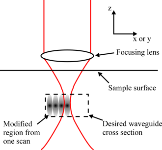
Working in the low repetition rate regime is therefore of greater interest, using corrective methods to control the waveguide cross section. Thus far, three techniques [2,3,4] have been suggested for fabricated waveguides with symmetric cross section while remaining in the low repetition rate regime. To date, we have focussed on the multi-scan technique since it is the most flexible of the proposed methods. In the multi-scan technique, the waveguide cross section is not determined either by thermal diffusion effects, or by the distribution of the electric field in the focal region. Instead, the desired waveguide cross section is built up by scanning the material repeatedly through the focus, each scan having an incremental shift of position relative to the last, as shown below.
Our work has so far has concentrated on device fabrication in a variety of materials, in particular active glasses for waveguide amplifier and laser applications, and also crystalline materials such as LiNbO3. We are also actively studying the modification process, and hope to gain further insight into the underlying fundamental physics.
Erbium and Erbium-Ytterbium doped Glasses
A significant amount of our work has been on fabricating waveguides in Er-doped Oxyfluoride silicate glasses. Oxyfluoride silicate glasses have several characteristics which make them promising candidates for use as gain materials such as broad gain bandwidths, large emission cross sections, a long upper state lifetime, and high structural stability and compatibility.
Initially our work was done using a 5 kHz fabrication laser (Spectraphysics Hurricane). Optimisation of the fabrication parameters enabled us to reduce insertion losses from 30+ dB down to 4.3 dB, exhibiting an internal gain of 1.7 dB for a 1.85 cm long waveguide. [5,6]


In collaboration with the Politecnico di Milano, we fabricated waveguides using a 600 kHz repetition rate laser (High-Q Femtonova). This enabled us to produce much higher quality waveguides with lower propagation losses and better mode-matching to telecoms fibres. The optimal waveguide exhibited a background insertion loss (excluding ground state absorption) of only 1.2 dB, and a corresponding fibre-fibre net gain of 0.73 dB for a 10mm long waveguide [7].


Bismuth doped Glass
Currently there are no convenient, efficient optical amplifiers suitable for WDM covering the second telecommunications window around 1.3 µm. The Praseodymium ion requires a low phonon glass host, inconvenient pump wavelengths and has a low quantum efficiency. Bismuth-ion doped glass has been shown to have extremely broad fluorescence and gain around 1.3 µm with several hundred nms of bandwidth [8]. Bi-doped glasses are therefore of great interest as a broadband gain medium. The potential for ultra broadband amplifiers and mode-locked lasers using the Bismuth ion is particularly promising.
Again, in collaboration with the Politecnico di Milano we fabricated waveguides in Bi-doped silicate glass using a pulse repetition rate of 600 kHz. We investigated both single and multi-scan fabrication in order to assess the optimal technique for this material and fabrication laser.
High quality waveguides were fabricated using both single and multi-scan fabrication with total insertion losses of 1.9 dB and 2.0 dB respectively. Images of the waveguide facet, corresponding refractive index profile, and guided mode profile are shown below. Fluorescence spectra are also shown for two excitation wavelengths of 810 nm and 980 nm. These results appear in our recent Optics Express paper [9].


Lithium Niobate
Lithium niobate (LiNbO3) has excellent acousto-optic, electro-optic, and nonlinear optical properties. For these reasons, it has long been used for active optical applications such as free space acousto-optic and electro-optic modulators and parametric amplification. In addition to these free space applications, integrated optical devices have also been fabricated using LiNbO3. Moving to an integrated optical platform can provide a number of benefits such as reduced device size and increased nonlinear interaction due to small mode confinement and longer interaction lengths. Examples of integrated optical devices fabricated using LiNbO3 include rf spectrum analyzers, electro-optic modulators, and wavelength converters. Traditionally, LiNbO3 waveguides are fabricated using either titanium in-diffusion or annealed proton exchange processes. These processes may either be performed across the whole of the LiNbO3 substrate to fabricate planar waveguides, or in selected regions only using masks defined through photolithography to create channel waveguides. The development of new fabrication techniques using LiNbO3 is therefore of great interest since it may open up new areas of device design and fabrication.
Initially, we fabricated waveguides in LiNbO3 using a 5 kHz repetition rate laser and were the first group to observe guiding at 1550 nm [10]. Two distinct types of waveguide were observed, which we define as Type I and Type II waveguides. Type I show guiding around a region of optical damage which was fabricated using a high pulse energy, and Type II which guide in the central modified region but which are fabricated using a lower pulse energy. Only Type I waveguides exhibited enough refractive index modification to support a mode at 1550 nm, and the quality of guiding quickly diminished as the index modification relaxed out.
We have conducted subsequent work in collaboration with the Politecnico di Milano, using a 600 kHz repetition rate. High quality low-loss waveguides were fabricated using the multiscan technique. These waveguides are long-lasting and support single mode guiding at 1550 nm.
References:
[2] R. Osellame, S. Taccheo, M. Maríangoni, R. Ramponi, P. Laporta, D. Polli, S. De Silvestri, and G. Cerullo, "Femtosecond writing of active optical waveguides with astigmatically shaped beams ," J. Opt. Soc. Am. B 20, 1559-1567 (2003)
[8] Y. Fujimoto and M. Nakatsuka, "Optical Amplification in bismuth-doped silica glass," Appl. Phys. Lett. 82,3325-3326 (2003)